
 On Tuesday, the University of Wisconsin-Madison gave us all a glimpse of the future of microelectronic devices when they reported a breakthrough in the development of a next generation technology – graphene nanoribbons (GNRs). This new technology promises to be a major advance in semiconductors with performance that is described as “dramatically” faster while simultaneously exhibiting better energy-efficiency properties.
See more about this breakthrough and learn why scientists are so excited about it…
Graphene is a material that is only one atom-thick, yet possesses “extraordinary” properties. According to the Science Daily, labs around the country have been studying the properties of graphene for quite some time now and many believe that it can, in essence, turbocharge microprocessor performance for the next generation of technology products.
As exciting as graphene appears to be – with performance properties well exceeding any existing microprocessor technology – researchers have been bedeviled by challenges related to fabricating the technology in a large-scale production environment. Simply put, to be useful in microelectronics, the material must be fabricated in ultra-narrow strips called nanoribbons which are then incorporated into microprocessors. Up until now, no one has figured out a good way to mass-produce nanoribbons of a sufficient quality for use in microprocessors.

Semiconductor Research Breakthrough
We learned on Tuesday that researchers at the University of Wisconsin-Madison have cracked the code, coming up with a mass-scale fabricating system that uses chemicals to stimulate an organic growth process. In essence, the researchers have figured out a way to “grow” graphene nanoribbons directly onto a conventional germanium semiconductor wafer.
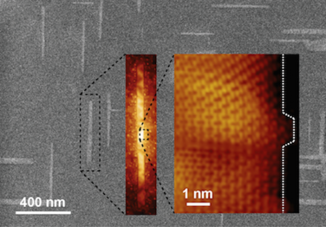
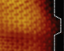
Credit: Arnold Research Group and Guisinger Research Group
According to the report, the invention of this new fabricating process will allow manufacturers to easily incorporate graphene nanoribbons into hybrid integrated circuits. Beyond the fact that this new fabricating process is easily scalable, it also is said to be compatible with existing microprocessor manufacturing processes.
Uses for Industry and Military
Uses for GNR technology are widely varied and include industrial and military applications. For example, GNR technology can be used to create sensors to detect chemical and biological species.
Associate professor of materials science and engineering at UW-Madison Michael Arnold and Ph.D. student Robert Jacobberger, along with collaborators published their findings in the August 10th edition of Nature Communications. Science journals around the world are trumpeting the news.
“Graphene nonoribbons that can be grown directly on the surface of a semiconductor like germanium are more compatible with planar processing that’s used in the semiconductor industry,” Arnold said. “And so there would be less of a barrier to integrating these really excellent materials into electronics in the future.”
Taking the Silicon Out of Silicon Valley
Even if you don’t live in Silicon Valley, most in our industry are familiar with the fact that silicon is the semiconducting material of choice for today’s microprocessors. But graphene, which is essentially a sheet of carbon atoms only one atom thick, is substantially better than silicon at both conducting electricity and efficiently dissipating heat.
In order to use graphene in a semiconducting application, where current is alternately switched on and off, it must be in the form of nanoribbons that are less than 10 nanometers wide. (Note: a nanometer is one billionth of a meter or 0.000000001 meter.) The report also notes that the nanoribbon must have smooth, well-defined edges (called “armchair” edges.)
Bottoms-Up Toast to the Bottom-Up Method
Existing fabricating methods for nanoribbons involve lithographic techniques that essentially cut larger graphene sheets into nanoribbons. However, according to the report, this method (called the “top-down” method) is imprecise and usually leaves rough edges on the nanoribbon.
The UW-Madison researchers have pioneered a “bottom-up” method which uses a chemical vapor deposition process to grow the ultra-narrow nanoribbons directly on the germanium wafer. The resulting nanoribbons are extremely narrow with straight and smooth armchair edges.
Calling Mr. Wizard
How does it do that? Since we’re not scientists – we’re going to quote directly from the report that explains the process:
In this process, the researchers start with methane, which adsorbs to the germanium surface and decomposes to form various hydrocarbons. These hydrocarbons react with each other on the surface [of the germanium wafer], where they form graphene.
The researchers also found that by controlling the rate and the time of the growth process, they can precisely control the width of the nanoribbons.
“What we’ve discovered is that when graphene grows on germanium, it naturally forms nanoribbons with these very smooth, armchair edges,” Arnold says in the report. “The widths can be very, very narrow and the lengths of the ribbons can be very long, so all the desirable features we want in graphene nanoribbons are happening automatically with this technique.”
As you might suspect, the researchers are applying for a patent on the technology. Support for the research was through the Department of Energy’s Basic Energy Sciences program.
See more on this amazing scientific breakthrough in semiconductor technology at Science Daily…


Leave a Reply